| Sign In | Join Free | My infospaceinc.com |
|
| Sign In | Join Free | My infospaceinc.com |
|
| Categories | Semiconductor Equipment |
|---|---|
| Brand Name: | ZMSH |
| Model Number: | Wafer Orientation Instrument |
| Certification: | rohs |
| Place of Origin: | CHINA |
| MOQ: | 3 |
| Price: | by case |
| Payment Terms: | T/T |
| Supply Ability: | 1000pcs per month |
| Delivery Time: | 3-6 months |
| Packaging Details: | package in 100-grade cleaning room |
| X-ray System: | X-ray Tube |
| Sample Size: | Wafer: 2–12 inch; Ingot: ≤200 mm (diameter) × 500 mm (length) |
| Angular Range: | θ: -10° to +50°, 2θ: -10° to +110° |
| Orientation Accuracy: | ±10″–±30″ (high-precision models: ±3″) |
| Multi-axis Motion: | X/Y/Z-axis positioning, 360° rotation ±15°, tilt control |
| Scanning Speed: | Full orientation in 10 sec (fully automated) |
| Applications: | Semiconductor Manufacturing, Optical Material Processing |
| Company Info. |
| SHANGHAI FAMOUS TRADE CO.,LTD |
| Verified Supplier |
| View Contact Details |
| Product List |

XRD-Based Wafer Orientation Instrument for High-Precision Cutting Angle Determination
A wafer orientation instrument is a high-precision device based on X-ray diffraction (XRD) technology, designed for semiconductor and optical material industries to determine crystal lattice orientation and cutting angles. Its core components include:
| Parameter Category | Parameter | Specifications/Description |
| X-ray System | X-ray Tube | Copper (Cu) target, focal spot 0.4×1 mm, air-cooled |
| X-ray Voltage/Current | 30 kV, 0–5 mA adjustable | |
| Detector Type | Geiger-Müller tube (low energy) or scintillation counter (high energy) | |
| Time Constant | 0.1/0.4/3 sec adjustable | |
| Goniometer | Sample Size | Wafer: 2–12 inch; Ingot: ≤200 mm (diameter) × 500 mm (length) |
| Angular Range | θ: -10° to +50°, 2θ: -10° to +110° | |
| Orientation Accuracy | ±10″–±30″ (high-precision models: ±3″) | |
| Angular Resolution | Minimum reading: 1″ (digital) or 10″ (scale) | |
| Scanning Speed | Full orientation in 10 sec (fully automated) | |
| Automation & Control | Sample Stage | V-groove (2–8 inch wafers), edge/OF alignment, 1–50 kg capacity |
| Multi-axis Motion | X/Y/Z-axis positioning, 360° rotation ±15°, tilt control | |
| Interface | PLC/RS232/Ethernet, MES-compatible | |
| Physical Specifications | Dimensions | 1130×650×1200 mm (L×W×H) |
| Weight | 150–300 kg | |
| Power Requirements | Single-phase 220V±10%, 50/60 Hz, ≤0.5 kW | |
| Noise Level | <65 dB (operating) | |
| Advanced Features | Closed-loop Tension Control | Real-time monitoring, 0.1–1.0 MPa tension regulation |
| AI-driven Optimization | Defect detection, predictive maintenance alerts | |
| Multi-material Compatibility | Supports cubic (Si), hexagonal (sapphire), and asymmetric crystals (YAG) |
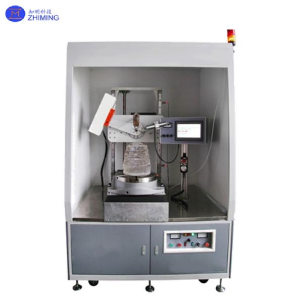
The device operates through X-ray diffraction and Omega scanning technologies:
1. X-ray Diffraction:
2. Omega Scanning:
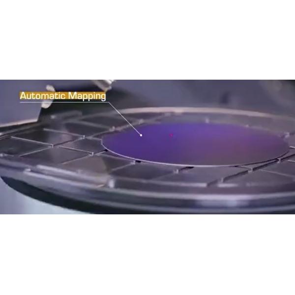
3. Automated Control:
Feature | Description | Technical Parameters/Case Studies |
Ultra-High Precision | Omega scanning accuracy ±0.001°, Rocking Curve FWHM resolution <0.005° | Silicon carbide wafer cutting error ≤±0.5° |
High-Speed Measurement | Single-scan acquisition of all crystallographic data, 200× faster than manual | Silicon wafer batch testing: 120 wafers/hour |
Multi-Material Compatibility | Supports cubic (Si), hexagonal (sapphire), and asymmetric crystals (YAG) | Applicable materials: SiC, GaN, quartz, garnet |
AI Integration | Deep learning algorithms for defect detection, real-time process optimization | Defect sorting reduces scrap rate to <1% |
Modular Design | Expandable X-Y platform for 3D mapping or EBSD integration | Silicon wafer dislocation density detection ≤100 cm⁻² |

1. Semiconductor Manufacturing:
2. Optical Material Processing:
3. High-Temperature Alloys & Ceramics:
4. Research & Quality Control:
1. Q: How to calibrate a wafer orientation instrument?
A: Calibration involves aligning the X-ray source and detector using reference crystals, typically requiring <0.001° angular accuracy and automated software adjustments for precision.
2. Q: What is the typical accuracy of a wafer orientation instrument?
A: High-end models achieve ±0.001° precision, critical for semiconductor wafer cutting and crystal defect analysis in industries like photovoltaics and advanced ceramics.
Tags: #Wafer Orientation Instrument, #XRD-Based, #Sapphire, #SiC, #High-Precision Cutting, # Angle Determination

|
 VIS-NIR Camera CCD Contour-IR Contour-M Digital Camera 400-1700nm Multispectral Camera
VIS-NIR Near-infrared CMOS Digital Camera CONTOUR-IR Multispectral Camera 400-1700nm
40 GHz Multi-Band Lithium Niobate Phase Modulator LNP6118 1310 Nm-1550 Nm
Automatic Double Cavity Semiconductor Fast Annealing Furnace Compatible With 6inch 8inch 12inch Wafer Heat Treatment Equipment 200-1300℃
UV Laser Marking Machine 355nm Wavelength 3W-20W Laser Power ±0.01mm Positioning Accuracy
Fiber Laser Marking Machine 20W-100W for Marking on Stainless Steel/Components
6inch-12inch SiC Substrate Laser Separation System Machine Wafers Customized
End-Pumped Laser Marking Machine 6W-30W High-Precision Marking 1064nm Wavelength
CO₂ Laser Marking Machine CO₂ Laser Fully Automatic Image & Text Engraving
CO₂ Laser Cutting Machine 40W-600W Positioning Accuracy±0.05mm
VIS-NIR Camera CCD Contour-IR Contour-M Digital Camera 400-1700nm Multispectral Camera
VIS-NIR Near-infrared CMOS Digital Camera CONTOUR-IR Multispectral Camera 400-1700nm
40 GHz Multi-Band Lithium Niobate Phase Modulator LNP6118 1310 Nm-1550 Nm
Automatic Double Cavity Semiconductor Fast Annealing Furnace Compatible With 6inch 8inch 12inch Wafer Heat Treatment Equipment 200-1300℃
UV Laser Marking Machine 355nm Wavelength 3W-20W Laser Power ±0.01mm Positioning Accuracy
Fiber Laser Marking Machine 20W-100W for Marking on Stainless Steel/Components
6inch-12inch SiC Substrate Laser Separation System Machine Wafers Customized
End-Pumped Laser Marking Machine 6W-30W High-Precision Marking 1064nm Wavelength
CO₂ Laser Marking Machine CO₂ Laser Fully Automatic Image & Text Engraving
CO₂ Laser Cutting Machine 40W-600W Positioning Accuracy±0.05mm

