| Sign In | Join Free | My infospaceinc.com |
|
| Sign In | Join Free | My infospaceinc.com |
|
| Categories | MOS Capacitors |
|---|---|
| Place of Origin: | Shaanxi, China |
| Chip Dimensions: | 0.55 × 0.55 × 0.18 mm (±25 µm); custom geometry up to 4:1 aspect ratio |
| Payment Terms: | L/C,D/A,D/P,T/T |
| CTE Match: | Silicon 2.6 ppm/°C, matched to GaN/SiC power substrates |
| Mounting Type: | Wire Bondable / AuSn Eutectic / Solder / Conductive Epoxy |
| Operating / Storage Temperature: | -55°C to +200°C / -65°C to +150°C |
| Brand Name: | Hoan |
| Delivery Time: | 5-7 working days for stock, 3-4 weeks for production |
| Certification: | ISO 9001:2015, RoHS |
| Capacitance Matching: | Sub-1% matched sets across wafer / wafer-to-wafer (digital wafer map) |
| Model Number: | HACC221S100V502 |
| Metallization: | TiW-Au top (≥2.5 µm Au) / TiW-Pt-Au backside (Au-only available) |
| MOQ: | 10 Pieces |
| Company Info. |
| HongAn Microwave Co., Ltd. |
| Verified Supplier |
| View Contact Details |
| Product List |
The HACC221S100V502 is a 220 pF ±10% single-layer MOS (metal-oxide-semiconductor) capacitor rated at 100 V DC, fabricated on float-zone silicon (>1000 Ω·cm) with 300 nm-class thermal SiO2 dielectric and TiW-Au / TiW-Pt-Au metallization. Standard chip outline is 0.55 mm × 0.55 mm × 0.18 mm (±25 µm). It is engineered for wide-bandgap power modules where pair-to-pair capacitance symmetry and thermo-mechanical reliability under power cycling determine circuit performance.
Because the silicon MOS structure is formed directly on a single-crystal silicon substrate, its coefficient of thermal expansion (CTE, 2.6 ppm/°C) is inherently close to that of silicon-carbide and GaN-on-SiC power devices — an advantage over alumina-based ceramic capacitors when co-packaged on power substrates.
| Nominal Capacitance | 220 pF ±10% (1 kHz, 1.0 Vrms); matched sets with <1% spread available |
| Rated Voltage | 100 V DC |
| Dielectric Withstanding Voltage | 250 V DC (250% rated, 5 s, 100% tested) |
| Temperature Coefficient (TCC) | +35 ppm/°C over -55°C to +200°C |
| Dissipation Factor | ≤0.15% at 1 kHz, 1.0 Vrms |
| Q Factor | >2000 at 1 MHz; >200 at 1 GHz |
| ESR at 1 GHz | <0.1 Ω |
| Intrinsic Chip ESL | <0.05 nH (de-embedded); chip-level SRF >1.5 GHz; system SRF >500 MHz with 0.5 mm Au bond wire |
| Leakage Current | <10 nA at 25°C; <500 nA at 200°C (at rated voltage) |
| Insulation Resistance | ≥104 MΩ at rated voltage, 25°C |
| ESD Tolerance | >2 kV HBM, Class 2 per JESD22-A114 |
| Operating / Storage Temperature | -55°C to +200°C / -65°C to +150°C |
| Standard Die Size | 0.55 × 0.55 × 0.18 mm (±25 µm); custom geometry, aspect ratio up to 4:1 |
| Metallization | TiW-Au top (≥2.5 µm Au, wire bondable); TiW-Pt-Au backside (AuSn / solder / silver epoxy) or Au-only backside |
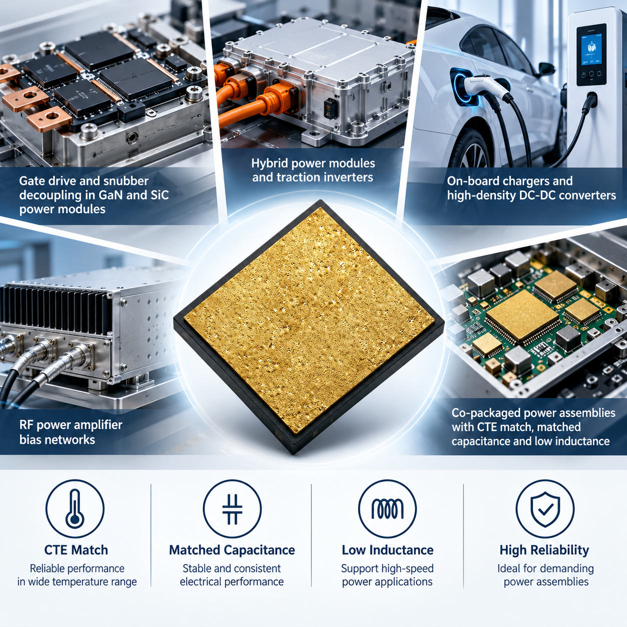
Gate drive and snubber decoupling in GaN and SiC power modules; hybrid power modules and traction inverters; on-board chargers and high-density DC-DC converters; RF power amplifier bias networks; and any co-packaged power assembly where CTE match, matched capacitance and low inductance are required.

|
 Ultra High SRF 100pF 25V MOS Capacitor Conductive Silicon Substrate Direct Grounding Single Layer RF Chip
Ultra-Low Leakage 150pF 100V MOS Capacitor High Dielectric Breakdown Strength Extreme Thermal Endurance SLC Chip
Custom Multi Capacitor Array 4 Channel 100pF 30V MOS Capacitor 100 Percent Wafer Level Tested SLC Chip
Miniaturized High-Density 220pF 30V MOS Capacitor Exceptional High-Frequency Stability Wafer-Level Custom SLC Chip
High-K Dielectric 330pF 25V MOS Capacitor Ultra-Low Phase Noise Wire Bondable Single Layer Chip for VCO PLL Circuits
Custom High Breakdown Voltage Low Leakage 1000 pF MOS Capacitor Ultra Stable TCC Wire Bondable Chip for RF Bypass
Ultra Small 0.40mm Bare Die Radiation Hardened 47pF 50V MOS Capacitor Zero Piezoelectric Noise Single Layer Chip
Custom High Q Ultra-Low ESL 470 pF MOS Capacitor Wire Bondable Single Layer Chip for RF Microwave Circuits
Zero Dielectric Memory 1000pF 80V MOS Capacitor Ultra-Linear CV Characteristics Paraelectric SiO2 Single Layer RF Chip
Low Dissipation Factor 50pF 50V MOS Capacitor Custom Metal Metallization SLC Chip for RF Power Packaging
Ultra High SRF 100pF 25V MOS Capacitor Conductive Silicon Substrate Direct Grounding Single Layer RF Chip
Ultra-Low Leakage 150pF 100V MOS Capacitor High Dielectric Breakdown Strength Extreme Thermal Endurance SLC Chip
Custom Multi Capacitor Array 4 Channel 100pF 30V MOS Capacitor 100 Percent Wafer Level Tested SLC Chip
Miniaturized High-Density 220pF 30V MOS Capacitor Exceptional High-Frequency Stability Wafer-Level Custom SLC Chip
High-K Dielectric 330pF 25V MOS Capacitor Ultra-Low Phase Noise Wire Bondable Single Layer Chip for VCO PLL Circuits
Custom High Breakdown Voltage Low Leakage 1000 pF MOS Capacitor Ultra Stable TCC Wire Bondable Chip for RF Bypass
Ultra Small 0.40mm Bare Die Radiation Hardened 47pF 50V MOS Capacitor Zero Piezoelectric Noise Single Layer Chip
Custom High Q Ultra-Low ESL 470 pF MOS Capacitor Wire Bondable Single Layer Chip for RF Microwave Circuits
Zero Dielectric Memory 1000pF 80V MOS Capacitor Ultra-Linear CV Characteristics Paraelectric SiO2 Single Layer RF Chip
Low Dissipation Factor 50pF 50V MOS Capacitor Custom Metal Metallization SLC Chip for RF Power Packaging

