| Sign In | Join Free | My infospaceinc.com |
|
| Sign In | Join Free | My infospaceinc.com |
|
| Categories | PCB Design |
|---|---|
| MOQ: | No MOQ |
| Supply Ability: | 100,000 pieces/month |
| Packaging Details: | ESD Protective Packaging/Customization |
| Delivery Time: | 5-25 working days(varies by product) |
| Place of Origin: | China |
| Price: | Quote based on your specs |
| Payment Terms: | T/T |
| Company Info. |
| Studio Technology Co., Ltd. |
| Verified Supplier |
| View Contact Details |
| Product List |

Signal integrity and EMI compliance are critical for reliable electronic products—especially in applications with high-speed interfaces, wireless connectivity, or regulatory certification requirements. Studio Electronics offers PCB Design with signal integrity and EMI optimization built into every project. As a specialized provider of PCB assembly in China, our professional PCB layout engineers use best practices in impedance control, differential routing, and EMI mitigation to ensure your boards meet both performance requirements and regulatory standards. We design, prototype, and validate before volume production.
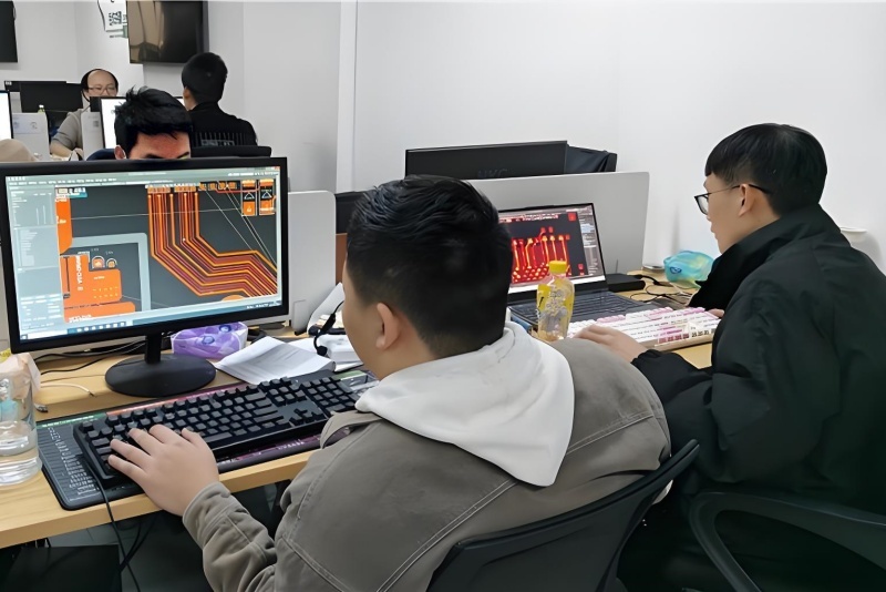
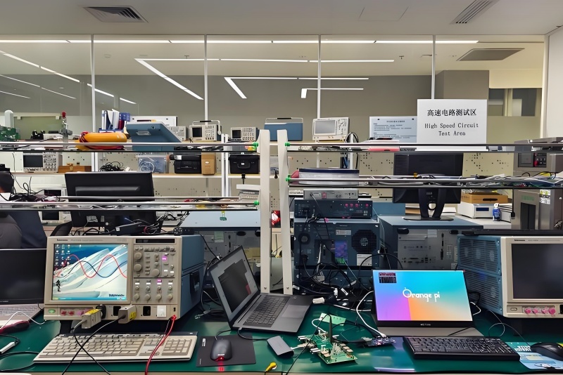
| Challenge | Design Strategy | Benefit |
|---|---|---|
| Reflections | Impedance-controlled routing; termination resistors | Clean signal edges; stable data transmission |
| Crosstalk | Controlled spacing; guard traces; layer design | Minimal signal coupling; reduced interference |
| EMI/RFI | Proper shielding; ground planes; filtering | Regulatory compliance; reduced emissions |
| Power Noise | PDN optimization; decoupling capacitors | Stable power; reduced ripple |
| High-Speed Interfaces | Differential routing; length matching | USB/HDMI/PCIe performance |

Stage 1: SI Requirements Analysis
We review your interface types, speeds, and EMI compliance targets.
Signal integrity requirements are documented before layout begins.
Stage 2: Stack-up & Routing
Layer stack-up is designed for impedance control. Critical nets are
routed with impedance control, differential pairing, and length
matching. Ground planes are designed for low-impedance return
paths.
Stage 3: EMI Mitigation
EMI mitigation techniques are applied throughout the design:
Stage 4: Design Review & Analysis
Signal integrity analysis validates timing and impedance. Design is
reviewed against EMI best practices.
Stage 5: Prototype Validation
We fabricate 5-10 samples and assemble them on our 12 automated SMT
lines. Prototypes undergo functional testing and signal integrity
validation. Samples are shipped to you for confirmation.


Studio delivers PCB Design—signal integrity and EMI optimization for reliable, compliant products.

|
 Robust PCB Design Thermal / Mechanical Analysis Custom Circuit Design
One Stop PCB Design And Fabrication OEM PCB Turnkey Assembly
Full Turnkey PCB Layout Design ODM Circuit Board Design Service
OEM ODM SMT Assembly Service Small Volume PCB Assembly Professional
Integrated Custom PCB Design And Fabrication DFM For Manufacturability
Custom Circuit Board Design With DFM Optimized For Production
ODM PCB Design And Manufacturing Customized Printed Circuit Board Design
Custom PCB Design And Assembly SMT / Through Hole PCB Board Design
High Yield Circuit Board Design Low Volume PCB Circuit Design
Quality Assured PCB Board Design PCB Design Services Performance
Robust PCB Design Thermal / Mechanical Analysis Custom Circuit Design
One Stop PCB Design And Fabrication OEM PCB Turnkey Assembly
Full Turnkey PCB Layout Design ODM Circuit Board Design Service
OEM ODM SMT Assembly Service Small Volume PCB Assembly Professional
Integrated Custom PCB Design And Fabrication DFM For Manufacturability
Custom Circuit Board Design With DFM Optimized For Production
ODM PCB Design And Manufacturing Customized Printed Circuit Board Design
Custom PCB Design And Assembly SMT / Through Hole PCB Board Design
High Yield Circuit Board Design Low Volume PCB Circuit Design
Quality Assured PCB Board Design PCB Design Services Performance

