| Sign In | Join Free | My infospaceinc.com |
|
| Sign In | Join Free | My infospaceinc.com |
|
| Categories | PCB Design |
|---|---|
| MOQ: | No MOQ |
| Place of Origin: | China |
| Supply Ability: | 100,000 pieces per month |
| Packaging Details: | ESD Protective Packaging/Customization |
| Delivery Time: | 5-25 working days(varies by product) |
| Price: | Quote based on your specs |
| Payment Terms: | T/T |
| Company Info. |
| Studio Technology Co., Ltd. |
| Verified Supplier |
| View Contact Details |
| Product List |

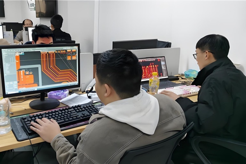
Advanced electronics demand advanced PCB design—High-Speed Digital Interconnect (HDI), microvias, buried vias, and fine-pitch routing for the most demanding applications. Studio Electronics offers Advanced PCB Design with high-speed and HDI expertise, handling designs that push the boundaries of PCB technology. As a premier provider of PCB assembly in China, our professional PCB layout engineers specialize in HDI designs with microvias, sequential lamination, and impedance-controlled routing. We design for both performance and production, with prototypes built, tested, and shipped for customer confirmation.
| Design Element | Our Capability | Application |
|---|---|---|
| HDI Design | Microvias; buried vias; sequential lamination | High-density; compact devices |
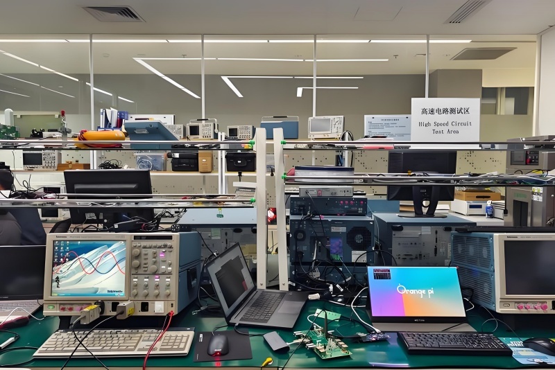
| High-Speed Interfaces | USB; HDMI; PCIe; DDR; Ethernet | Performance-critical applications |
| Impedance Control | ±5% tolerance; controlled stack-up | Signal integrity assurance |
| Fine-Pitch Routing | 3mil trace/space capability | Dense component placement |
| Multi-Layer Stack-up | Up to 20 layers; controlled impedance | Complex, high-performance designs |
Stage 1: Requirements Analysis
We review your advanced design requirements—HDI structure,
high-speed interfaces, impedance control targets, and production
goals.
Stage 2: Advanced Design
Our engineers create the design with HDI and high-speed expertise:
Stage 3: Advanced DFM Review
Design is verified against advanced fabrication and assembly
capability. HDI design rules, via structures, and material
selections are optimized.
Stage 4: Prototype Build
We fabricate 5-10 sample boards and assemble them on our 12
automated SMT lines with ±25μm accuracy.
Stage 5: Validation & Customer Approval
Prototypes undergo AOI, X-Ray, ICT, and functional testing. Samples
are shipped for your confirmation.

Studio delivers Advanced PCB Design—high-speed and HDI expertise for the most demanding applications.

|
 Robust PCB Design Thermal / Mechanical Analysis Custom Circuit Design
One Stop PCB Design And Fabrication OEM PCB Turnkey Assembly
Full Turnkey PCB Layout Design ODM Circuit Board Design Service
OEM ODM SMT Assembly Service Small Volume PCB Assembly Professional
Integrated Custom PCB Design And Fabrication DFM For Manufacturability
Custom Circuit Board Design With DFM Optimized For Production
ODM PCB Design And Manufacturing Customized Printed Circuit Board Design
Custom PCB Design And Assembly SMT / Through Hole PCB Board Design
High Yield Circuit Board Design Low Volume PCB Circuit Design
Quality Assured PCB Board Design PCB Design Services Performance
Robust PCB Design Thermal / Mechanical Analysis Custom Circuit Design
One Stop PCB Design And Fabrication OEM PCB Turnkey Assembly
Full Turnkey PCB Layout Design ODM Circuit Board Design Service
OEM ODM SMT Assembly Service Small Volume PCB Assembly Professional
Integrated Custom PCB Design And Fabrication DFM For Manufacturability
Custom Circuit Board Design With DFM Optimized For Production
ODM PCB Design And Manufacturing Customized Printed Circuit Board Design
Custom PCB Design And Assembly SMT / Through Hole PCB Board Design
High Yield Circuit Board Design Low Volume PCB Circuit Design
Quality Assured PCB Board Design PCB Design Services Performance

