| Sign In | Join Free | My infospaceinc.com |
|
| Sign In | Join Free | My infospaceinc.com |
|
| Categories | Electronics PCB Manufacturing |
|---|---|
| Price: | Quote based on your specs |
| Delivery Time: | 5-25 working days(varies by product) |
| Packaging Details: | ESD Protective Packaging/Customization |
| Place of Origin: | China |
| MOQ: | No MOQ |
| Payment Terms: | T/T |
| Supply Ability: | 100,000 pieces per month |
| Company Info. |
| Studio Technology Co., Ltd. |
| Verified Supplier |
| View Contact Details |
| Product List |

Overview
Zero-defect is not just a quality goal at Studio Electronics—it is a requirement enforced by 100% comprehensive testing of every board we produce. We offer zero-defect Electronics PCB Manufacturing backed by full inspection coverage using AOI, SPI, 3D X-Ray, ICT, FCT, and Flying Probe testing. As a leading provider of PCB assembly in China, we apply rigorous testing protocols to every board, regardless of order size. Whether you need 10 prototypes or 10,000 production boards, each board is verified against your specifications at every stage—from material procurement and PCB fabrication through component assembly, testing, final assembly, and delivery.
Our Zero-Defect Manufacturing Process
| Stage | Process Steps | Testing Coverage |
|---|---|---|
| 1. Material Procurement | Sourcing PCB boards, electronic components, assembly materials | 100% incoming inspection; LCR testing; Brand authenticity verification |
| 2. PCB Fabrication | Bare board creation: etching, layering, drilling | Dimensional inspection; surface finish verification; 100% bare board testing |
| 3. Component Assembly | SMT and THT placement using automated instruments | 100% SPI before reflow; 100% AOI after placement; 100% X-Ray for hidden joints |
| 4. Testing & Quality Control | Functional tests and quality checks | 100% ICT; 100% FCT; 100% Flying Probe for small batches |
| 5. Final Assembly | Board integration; component connection; final verification | Functional verification of assembled product; 100% visual inspection |
| 6. Delivery | Protective packaging; customs clearance; on-time delivery | Packaging verification; shipping documentation review |

100% Testing Coverage – Every Board, Every Time
| Testing Stage | Equipment | What We Verify | Coverage |
|---|---|---|---|
| Pre-Reflow | 3D SPI | Solder paste volume, height, area | 100% of boards |
| Post-Reflow Visual | AOI | Component presence, polarity, alignment, solder joints | 100% of boards |
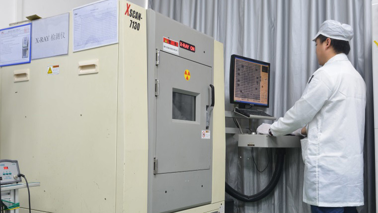
| Hidden Joint | 3D X-Ray | BGA, QFN voids, bridging, insufficient solder | 100% of boards |
| Electrical Validation | ICT | Component values (R, C, L); shorts/opens | 100% of boards |
| Functional Verification | FCT | Full board performance under simulated conditions | 100% of boards |
| Fixture-less Testing | Flying Probe | Rapid electrical verification for low volume PCB assembly | As required |

Advanced Equipment Supporting Zero-Defect Manufacturing
12 Fully Automated SMT Lines – High-speed placement with ±25μm accuracy; consistent, repeatable results across all boards
Automatic Wave Soldering – Programmable closed-loop control; ±1°C accuracy; reliable THT soldering
Programmable Automated Soldering Robots – ±0.05mm positional accuracy; precision selective soldering
3D SPI – Micron-level paste measurement; real-time feedback to screen printer
3D AOI – AI-assisted defect detection and classification; high-speed optical inspection
3D X-Ray – Automated void calculation; detects sub-10μm defects
Reliability Laboratory – Environmental testing including thermal shock, temperature cycling, damp heat, and vibration
How We Achieve Zero Defects
Prevention – DFM reviews identify potential issues before production; supplier quality management ensures component authenticity; 3D SPI prevents paste-related defects
Detection – Multi-layered inspection catches defects at the earliest possible stage; 100% coverage ensures no board escapes inspection
Correction – MES tracks all inspection data; when defects are detected, corrective action is triggered immediately; root cause analysis prevents recurrence
For low volume PCB assembly, we apply the most rigorous testing protocol—every board individually tested with full inspection coverage—because every unit is valuable and must perform to specification. Choose Studio for zero-defect Electronics PCB Manufacturing—where 100% testing ensures every board meets your specifications and performs reliably in the field.

|
 Agile PCB Design & Manufacturing Services Custom Electronic Assembly Prototype
Full Service Electronics PCB Manufacturing Sourcing To Shipping
Fast Turn Circuit Board Manufacturing Precision Electronic PCB Board Manufacturer
One Stop Turnkey PCB Electronics EMS Solutions Electronics Assembly Services
End To End Electronics Assembly Smart PCB Manufacturing Services
Complete Electronic Circuit Board Assembly Fab To Box Build
Precision PCB Manufacturing Assembly 12 SMT Lines / X Ray OEM
Smart Electronics PCB Manufacturing AI Powered PCB Assembly Manufacturer
AOI SPI ICT FCT Electronics Assembly Advanced Custom Circuit Board Manufacturers
Automated SMT Soldering Electronics PCB Manufacturing Circuit Board Manufacturing
Agile PCB Design & Manufacturing Services Custom Electronic Assembly Prototype
Full Service Electronics PCB Manufacturing Sourcing To Shipping
Fast Turn Circuit Board Manufacturing Precision Electronic PCB Board Manufacturer
One Stop Turnkey PCB Electronics EMS Solutions Electronics Assembly Services
End To End Electronics Assembly Smart PCB Manufacturing Services
Complete Electronic Circuit Board Assembly Fab To Box Build
Precision PCB Manufacturing Assembly 12 SMT Lines / X Ray OEM
Smart Electronics PCB Manufacturing AI Powered PCB Assembly Manufacturer
AOI SPI ICT FCT Electronics Assembly Advanced Custom Circuit Board Manufacturers
Automated SMT Soldering Electronics PCB Manufacturing Circuit Board Manufacturing

